
MATERIAL
- HOME
- MATERIAL
Examples of analysis – Material samples
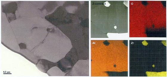
Analysis of ceramics with FIB processing Left: x40,000 TEM Right: Z contrast image, EDX area analysis
We provide FIB processing and analysis of semiconductors and ceramics. In addition to regular TEM analysis, we can perform electron diffraction imaging, line and area analysis with EDX, and HAADF-STEM imaging of Z-contrast images.
Superconducting Metal x3,000,000 TEM
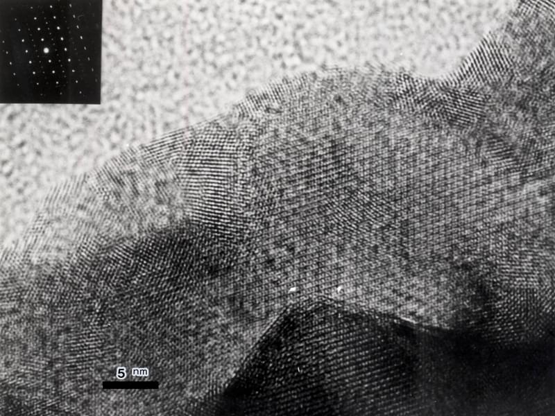
This is an expanded image of the edge of Y-Ba-Cu-O powder after the power was sprinkled and spread over a carbon-coated grid.
In this metal, crystalline lattices cross each other in a complex manner due to stacked crystals and grain boundary. From the electron diffraction patterns shown in the upper left corner, we can learn the crystal form and crystal orientation. Observation of the image along with the TEM images allows us to perform detailed structural analysis of the sample.
High resolving power observation of a carbon nanotube x300,000 TEM
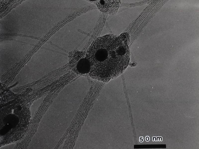
CNT, which was discovered with an electron microscope, is hoped today that it may have various properties, and is being studied around the world in search of additional utility.
Structural analysis of single-walled and multi-walled CNT can be directly observed with the transmission electron microscope.
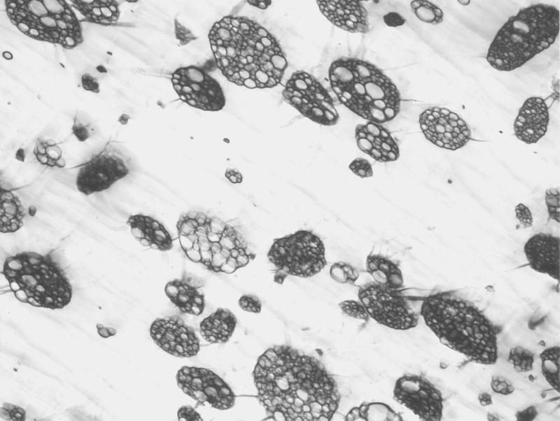
Observation of the liposomes’ multilayer structure using the negative staining method x200,000 TEM

Liposomes are spherical particles with a bilayer or multilayer lipid structure and have both hydrophobic and hydrophilic properties. They are used in many products such as drugs and cosmetics.
The layer structure can be observed by considering staining conditions and using the negative staining method.
HIPS x5,000
High-impact polystyrene. The internal rubber particles with the salami structure absorb the impact. Since rubber particles are soft and are difficult to be sliced thin at normal temperature, sectioning has to be performed in a frozen state at -100 ℃.
Polymer Particles x10,000
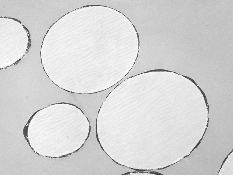
Sectioning allows observation of the surface condition of a thin metal layer.
It is difficult to slice thin because the hardness varies.
Cross section of a lens x15,000
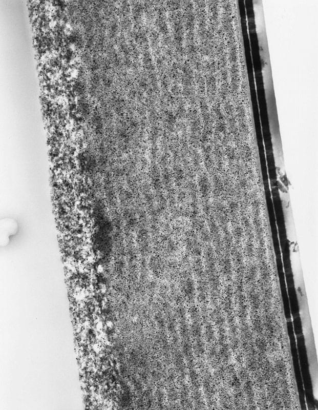
A section of a plastic lens was observed with a TEM. The thickness of the protective layer (metal) on the surface and the internal laminating condition are visible.